
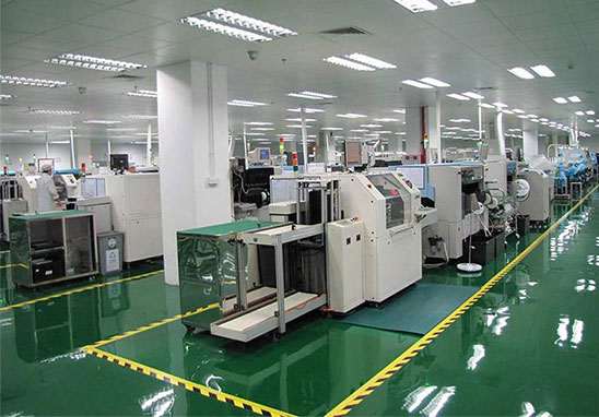
PCBFuture has smt assembling factory, which can provide the SMT assembly services for the smallest package 0201 components. It is support various processing ways such as turnkey PCB assembly and pcba OEM services. What inspections need to do before the SMT PCB processing?
1. The inspection of SMT components
The inspection items include: solderability, pin coplanarity and usability, which should be sampled by the inspection department. To test the solderability of components, we can use the stainless steel tweezers to clamp the component and immerse in a tin pot at 235±5℃ or 230±5℃, and take it out at 2±0.2s or 3±0.5s. We should check the condition of the welding end under the 20x microscope. It is required that more than 90% of the welding end of the components are wetted with tin.
Our SMT process workshop will do below apearance inspections:
1.1 checking the welding ends or pin surfaces of the components for oxidation or contamination visually or with a magnifying glass.
1.2 The nominal value, specification, model, accuracy, and external dimensions of the components should be consistent with the PCB requirements.
1.3 The pins of SOT and SOIC cannot be deformed. For multi-lead QFP devices with a lead pitch of less than 0.65mm, the coplanarity of the pins should be less than 0.1mm and we can inspection by the mounter optical inspection.
1.4 For PCBA that require cleaning for SMT patch processing, the mark of the components must not fall off after cleaning, and can not affect the performance and reliability of the components.
2 The PCB inspection
2.1 The PCB land pattern and size, solder mask, silk screen, and via hole settings should meet the design requirements of SMT printed circuit boards. We can check the pad spacing is reasonable, the screen is printed on the pad, and the via is made on the pad, etc.
2.2 The dimensions of the PCB should be consistent, and the dimensions, positioning holes, and reference marks of the PCB should meet the requirements of the production line equipment.
2.3 PCB allowable bending size:
2.3.1 Upward/convex: maximum 0.2mm/50mm length and maximum 0.5mm/the length of the whole PCB.
2.3.2 Downward/concave: maximum 0.2mm/50mm length and maximum 1.5mm/the length of the whole PCB.
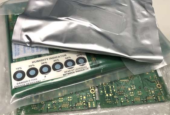
2.3.3 We should check the if PCB are contaminated or damp.
![]()
3 The precautions for SMT PCB process:
3.1 The technician wears the inspected electrostatic ring. Before plug-in, we should checks the electronic components of each order are free of errors/mixing, damage, deformation, scratches, etc.
3.2 The plug-in board of the PCB needs to prepare the electronic materials in advance, and note the direction of the capacitor polarity must be correct.
3.3 After the SMT printing operation is completed, check for defective products such as no missing insertion, reverse insertion, and misalignment, etc., and put the tin finished PCB into the next process.
3.4 Please wear an electrostatic ring before SMT PCB during PCB assembly process. The metal sheet should be close to the skin of the wrist and be well grounded. Work alternately with both hands.
3.5 The metal components such as USB, IF socket, shielding cover, tuner and network port terminal must wear finger cots when plugging in.
3.6 The position and direction of the components must be correct. The components should be flat against the board surface, and the elevated components must be inserted at the K foot .
3.7 If the material be inconsistent with the specifications on the SOP and BOM, it must be informed to the monitor or group leader in time.
3.8 The material should be handled with care. Do not continue to use the PCB with damaged components, and crystal oscillator cannot be used after it is dropped.
3.9 Please tidy and keep the work surface clean before working and get off work.
3.10 Strictly abide by the operating rules of the work area. PCB in the first inspection area, to-be-inspected area, defective area, maintenance area, and low-material area not allowed to random place.
4 Why choose PCBFuture for pcb assembly services?
4.1 The strength guarantee
4.1.1 Workshop: It has imported equipment, which can produce 4 million points per day. Each process is equipped with QC who can keep the PCB quality.
4.1.2 DIP production line: There are two wave soldering machines, and PCBFuture has more than dozens experienced employees with more than three years of experience. The workers are highly skilled and can weld various plug-in materials.
4.2 The quality assurance, high cost effective
4.2.1 High-end equipment can paste precision shaped parts, BGA, QFN, 0201 materials. It can also be used to the sample patch and placing bulk materials by hand.
4.2.2 Boths prototype pcb assembly service, volume pcb assembly services can be provide.
4.3 Rich experience in SMT PCB and soldering of PCB, and it is stable delivery time.
4.3.1 Accumulated services to thousands of electronics companies, involving SMT assembly service for various types of automotive equipment and industrial control motherboards. The PCB and PCB assembly are exported to Europe and the United States, and the quality be affirmed by customers.
4.3.2 Delivery on time. The normal 3-5 days if the materials are complete and solve the EQ, and small batches can also be shipped in a day.
4.4 Strong maintenance ability and good at after-sales service
4.4.1 The maintenance engineer has rich experience and they can repair defective PCBs caused by various patch welding. PCBFuture can ensure the connectivity rate of each PCB.
4.4.2 The customer service will respond at 24-hour and solve people’s order problems as quickly as possible.
Media Contact
Company Name: SHENZHEN KAISHENG PCB CO., Ltd.
Email: Send Email
Phone: 86-0752-8898101
Country: China
Website: https://www.pcbfuture.com/