
Shenzhen,Guangdong,China-October 14, 2026
What Is Selective Solder Bead Cleaning?
Selective solder bead cleaning uses a controlled brush path to treat designated PCB areas. Its suitability depends on the location of the bead, how firmly it is attached, and whether the tool can reach it without damaging the assembly.
The NSDTECH Selective Solder Bead Cleaning Machine offers programmable X/Y/Z motion, Gerber or PCB image import, and optional brush diameters from 10 to 30 mm.
These features support application-specific process setup. The final brush, path, and operating parameters should be validated using representative production boards.
Before-and-After Images: What Should They Demonstrate?
A useful comparison should show more than a cleaner-looking surface. It should help engineers determine whether the unwanted particles were removed and whether the surrounding assembly remained intact.
Before Cleaning
Capture the target area clearly enough to identify:
- The number and approximate size of visible solder beads.
- Their positions relative to component bodies, leads, and solder joints.
- Whether they are on exposed solder mask or trapped in a restricted area.
- Existing scratches, residue, or component damage.
Mark the intended cleaning area and nearby features that must remain untouched.
After Cleaning
Photograph the same location using the same magnification, lighting, and viewing angle.
Check the target area and nearby spaces for:
- Remaining solder beads.
- Particles displaced toward leads or connector openings.
- New scratches or solder mask damage.
- Bent leads, displaced components, or damaged markings.
- Detached brush fibers or other introduced debris.
A bead disappearing from the original location does not prove that it has left the PCB. Adjacent areas must also be inspected.
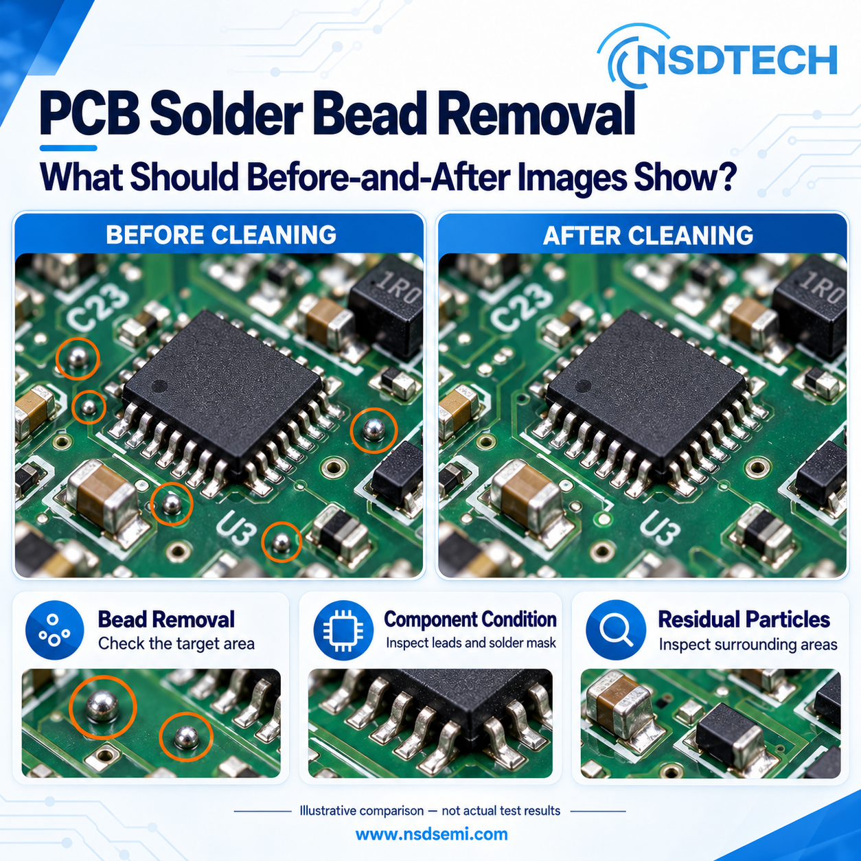
Suggested Before-and-After Image Layout
|
Image panel |
Recommended content |
Suggested label |
|
Before |
Actual sample image with unwanted beads marked |
Before: Solder Beads in Target Area |
|
After |
Same location following the cleaning trial |
After: Same Area Following Selective Cleaning |
|
Detail |
Magnified view of adjacent leads and solder mask |
Detail: Post-Cleaning Inspection |
Suggested caption:
“Matched microscope views of the same PCB area before and after a selective solder bead cleaning trial. Results apply to the tested board, brush, and process settings.”
Suggested image alt text:
“PCB solder bead removal before and after selective brush cleaning at the same inspection location.”
Use actual sample photographs for performance comparisons. Concept illustrations should be identified as illustrations rather than presented as measured cleaning results.
How to Select a Brush for PCB Solder Bead Removal
Brush selection should consider the target area, nearby components, bead adhesion, and the complete tool clearance.
1. Match Brush Diameter to the Accessible Area
A smaller brush can provide a more localized contact area. A larger brush can cover a broader exposed region, but requires more clearance.
The following table provides a starting point for sample evaluation, not a guaranteed application mapping.
|
Available brush diameter |
Possible evaluation starting point |
Main consideration |
|
10 mm |
Localized, accessible cleaning areas |
Confirm clearance for both bristles and holder |
|
15 mm |
Small exposed regions near populated areas |
Check bristle spread near neighboring components |
|
20 mm |
Medium-sized open cleaning regions |
Balance coverage with selective access |
|
25 mm |
Broader exposed PCB regions |
Avoid unnecessary contact with populated areas |
|
30 mm |
Large, unobstructed regions |
Confirm the full swept area remains clear |
A nominal brush diameter does not define the minimum usable gap. Bristle deflection, holder size, positioning variation, and component geometry also matter.
2. Evaluate Bristle Stiffness and Contact Depth
Softer bristles may reduce mechanical loading, but may not remove strongly attached particles. Stiffer bristles may increase removal force while also increasing the risk of surface damage or component disturbance.
Begin trials with conservative contact settings. Adjust one parameter at a time and inspect the result before increasing brushing intensity.
If a bead remains firmly attached, reassess the removal method rather than repeatedly increasing force.
3. Confirm Material and ESD Compatibility
Check the proposed brush material against the assembly’s electrostatic discharge control requirements.
Brush color alone does not establish ESD suitability. Confirm the brush specification, its compatibility with the equipment, and the required grounding arrangement.
Also evaluate bristle shedding, wear, and the possibility of transferring collected particles between boards.
4. Control Brush Condition
Include brush condition in routine process checks.
Replace or service the brush when wear, contamination, or deformation affects its contact footprint or cleaning consistency. A recipe validated with a new brush should not be assumed to remain effective with a heavily worn one.
How to Plan Component Avoidance
Component avoidance requires evaluating the complete moving tool, including its holder and deflected bristles.
Define Cleaning Areas and No-Contact Areas
Create a board-specific map identifying:
- Areas requiring solder bead removal.
- Component bodies and exposed leads.
- Connector openings and contact surfaces.
- Sensitive surfaces, openings, and unsupported board regions.
- Features that must remain outside the brush path.
These boundaries may be implemented through approved path programming and setup controls. Confirm the available software functions for the selected configuration.
Check Height as Well as Plan View
A path that appears clear in a top-down PCB image may still bring the brush holder into contact with a tall component.
Review component height data and inspect the actual assembly. Gerber data or a two-dimensional image alone may not describe every mechanical obstruction.
Validate Approach, Cleaning and Withdrawal
Check the complete motion sequence:
- Approach the target without crossing an obstruction at an unsafe height.
- Establish the approved brushing contact.
- Move through the validated cleaning path.
- Withdraw before transferring to the next location.
Confirm motion using the machine’s approved setup procedure and representative samples.
Support the PCB Properly
Board movement or deflection can change the brush contact depth. Check the support arrangement and confirm that the assembly remains stable during cleaning.
Machine positioning accuracy should not be treated as the required component clearance. Clearance must also account for board location, tool geometry, bristle spread, and process variation.
Where Is Selective Brush Cleaning Applicable?
Selective brushing is most promising when unwanted beads are accessible and can be removed without disturbing intended solder joints or nearby components.
|
PCB condition |
Application assessment |
|
Loose or lightly attached beads on exposed solder mask |
Candidate for a controlled sample trial |
|
Beads beside a component with adequate tool clearance |
Evaluate brush access and component avoidance |
|
Beads partly retained by flux residue |
Test adhesion and determine whether another cleaning process is needed |
|
Beads beneath a low-clearance package or enclosed shield |
Do not assume external brushing can reach them |
|
Solder bridges between leads |
Require an appropriate solder rework process |
|
Solder attached to an intended joint |
Assess as a soldering or rework issue before brushing |
|
Ionic contamination or widespread flux residue |
Requires a suitable cleanliness assessment and cleaning process |
|
Coated, bonded, or mechanically delicate regions |
Requires specific compatibility evaluation |
Cleaning Around a BGA Is Not Cleaning Under a BGA
Accessible particles near the outside of a BGA package may be evaluated for selective removal.
This does not establish access to particles underneath the package. Hidden contamination requires a suitable inspection and disposition method.
Solder Bead Removal Is Not Flux Cleaning
Removing visible metallic particles does not demonstrate that flux residues or ionic contamination have been removed.
If chemical cleanliness is a requirement, define a separate cleaning and verification process appropriate to the assembly.
Cleaning Does Not Replace Soldering Process Improvement
When solder beads recur, review the upstream process alongside the removal operation. Cleaning can address affected boards, while process investigation helps reduce repeated defects.
Recommended Sample Validation Procedure
Before introducing a cleaning recipe into production:
- Select representative samples.Include typical contamination and difficult but expected locations.
- Record the initial condition.Photograph target areas and document existing damage.
- Check tool access.Confirm brush, holder, component, and support clearances.
- Run controlled trials.Record brush specification, contact settings, path speed, and pass count.
- Inspect the complete result.Check particle removal, adjacent areas, component condition, and introduced debris.
- Perform additional checks where needed.Use appropriate electrical or functional testing when visual inspection cannot establish acceptability.
- Release a documented recipe.Record the board revision, approved settings, inspection criteria, and brush maintenance requirements.
Include particle collection and housekeeping in the evaluation. Confirm how removed debris is managed in the proposed equipment configuration.
Frequently Asked QuestionsCan one brush be used for every PCB?
Not necessarily. Different layouts, component heights, and contamination conditions may require different brushes or cleaning paths.
Is a smaller brush always safer?
No. A smaller brush may improve local access, but excessive contact force, unsuitable bristles, or poor path planning can still damage the assembly.
Can selective cleaning remove every solder bead?
No universal removal rate should be assumed. Results depend on accessibility, adhesion, surrounding geometry, and the validated process settings.
Are before-and-after photos enough to approve the process?
They are useful evidence, but may not reveal hidden particles, electrical damage, or chemical contamination. Approval should follow the product’s defined quality requirements.
What information should be provided for an application review?
Provide PCB images, close-up defect photographs, board dimensions, component height information, target cleaning areas, and the required production output. Representative physical samples help establish practical suitability.
Evaluate Your PCB Cleaning Application with NSDTECH
Effective selective solder bead removal starts with understanding the actual defect and the available tool access.
Share your PCB layout, solder bead photographs, and representative samples with NSDTECH to discuss brush selection, component clearance, and cleaning trials.
Learn more about the NSDTECH Selective Solder Bead Cleaning Machine and evaluate its suitability for your PCB production process.
About Us
As a global intelligent equipment &material provider, NSDTECH has continued to focus on SIX major fields: Semiconductor Packaging and Testing Equipment; Semiconductor Packaging and Testing Materials; AI+Vision Inspection; Automated Testing; Intelligent Manufacturing; PCBA Auxiliary Materials since 2011 for global customers. We provide customers with cost-effective to their total solutions requirement.
Media Contact
Company Name: Shenzhen Nsdtech Technology Co., Ltd.
Contact Person: Media Relations
Email: Send Email
Country: China
Website: https://www.nsdsemi.com/