Market Overview
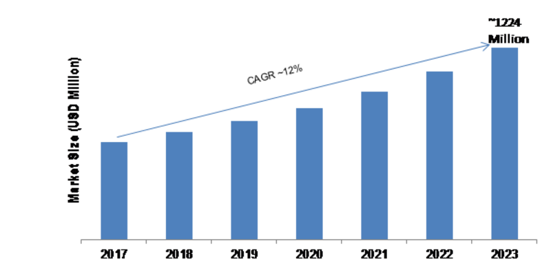
Market Research Future (MRFR), in its recently published report, asserts that the global GaAs wafers market 2020 is booming and expected to grow signficantly over the review period, recording a substantial market valuation from USD 625 million in 2017 up to USD 1224.3 million by 2023, and a healthy 12% CAGR in the forecast period.
Request Free Sample @ https://www.marketresearchfuture.com/sample_request/6473
Drivers and Restraints
The significant growth drivers for GaAs wafers market are growing acceptance of smartphones and rising dissemination of light emitting diode (LED) in general lighting. The introduction of IoT has been one of the major factors responsible for the increasing trend of the market. The technology has given rise to a need for high-frequency communication gadgets incorporated with GaAs based ICs.
Also, with various companies expanding their communication infrastructure, the need for GaAs based devices is going to rise, which in turn will trigger the expansion of the GaAs Wafer and Epi Wafer Market in the upcoming years. The demand for GaAs devices over various end-user industries such as aerospace &, defense, electronics and communications is increasing consequently is boosting the demand for GaAs Wafers globally. he rising internet penetration across the world, especially in developing countries such as India, china, and Brazil, has encouraged the demand for GaAs wafers. Subsequently, the demand for backhaul, base stations, and fiber-optic networks in wireless communication infrastructural development and Wi-Fi connectivity products have accelerated and hence support the growing deployment of the internet worldwide, which, consequently, is boosting the adoption of GaAs wafers.
Further, the development of mobile data and the wide adoption of IoT is fueling the requirement of Wi-Fi and other wireless communication devices. The increasing growth rates for such technologies and other products connected to wireless communications are aiding the implementation of GaAs wafers. Therefore, the demand for GaAs wafers for wireless communications networks will continue to upsurge during the forecast period. Furthemorer, another key factor driving the growth of the GaAs wafer market includes increasing adoption of 4G and 5G networks over the world. However, the limiting factor affecting the GaAs wafer industry include its high production cost.
Segmental Analysis
Based on the production method, the GaAs Wafers Market is segmented into Liquid encapsulated Czochralski (LEC), vertical gradient freeze (VGF), Molecular Beam Epitaxy (MBE), Metal-Organic Vapor Phase Epitaxy (MOVPE).
Based on the application, the GaAs wafers market is segmented into mobile devices, wireless communication, photovoltaic devices, optoelectronic devices, aerospace & defense, and others.
Regional Synopsis
The geographical analysis of the global GaAs wafers market has been conducted in four major regions, comprising the Asia Pacific, North America, Europe, and the rest of the world (Latin America, the Middle East and Africa). North America is slated to grow at a faster rate during the forecast period due to the presence of major vendors and growing adoption of new technologies and related services in the region. Asia-Pacific is anticipated to dominate the GaAs wafer market during the forecast period owing to growing number of smartphone users. Growing population, increasing number of semiconductor manufacturers, telecom industries, government initiatives to make smart cities, and increasing smartphone users are a few notable factors driving the GaAs wafer market in Asia-Pacific. China, Taiwan, Japan are estimated to dominate the GaAs wafer market in Asia-Pacific. Whereas, South Korea, India, are expected to grow at a fast rate during forecast period. Europe is expected to remain steady during forecast period due to increasing use of GaAs wafers in consumer electronics applications.
Competitive Overview
The key market players operating in the global GaAs wafers market as identified by MRFR are Global Communication Semiconductors, LLC (US), Advanced Wireless Semiconductor Company (Taiwan), WIN Semiconductors Corporation (Taiwan), Ommic S.A. (France), AXT Inc. (US), Century Epitech Co Ltd. (China), Sumitomo Electric Semiconductor Materials Inc. (US), Intelligent Epitaxy Technology, Inc. (US), Powerway Advanced Material Co., Ltd. (China), Freiberger Compound Materials GmbH (Germany) among others.
Other players in GaAs market are United Monolithic Semiconductors (France), Qorvo, Inc. (US), and Visual Photonics Epitaxy Co, Ltd. (Taiwan) IQE plc (UK), among others.
Get Report Details @ https://www.marketresearchfuture.com/reports/gaas-wafer-market-6473
About Market Research Future:
At Market Research Future (MRFR), we enable our customers to unravel the complexity of various industries through our Cooked Research Report (CRR), Half-Cooked Research Reports (HCRR), Raw Research Reports (3R), Continuous-Feed Research (CFR), and Market Research & Consulting Services.
Media Contact
Company Name: Market Research Future
Contact Person: Abhishek Sawant
Email: Send Email
Phone: +1 646 845 9312
Address:Market Research Future Office No. 528, Amanora Chambers Magarpatta Road, Hadapsar
City: Pune
State: Maharashtra
Country: India
Website: https://www.marketresearchfuture.com/reports/gaas-wafer-market-6473

